Well, we all know that chip designing to chip manufacturing includes several long processes and steps. VLSI BACKEND i.e Physical Design is one such process.
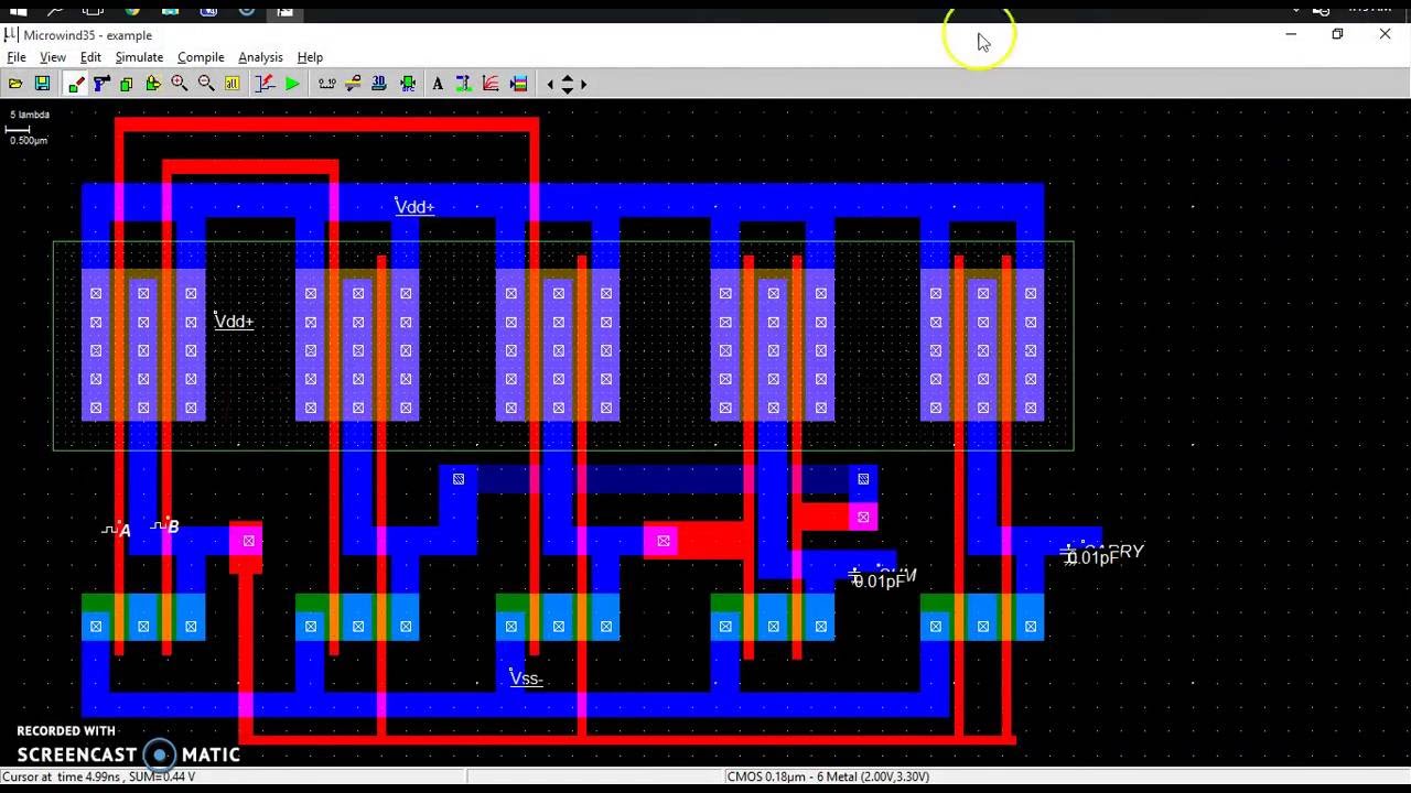
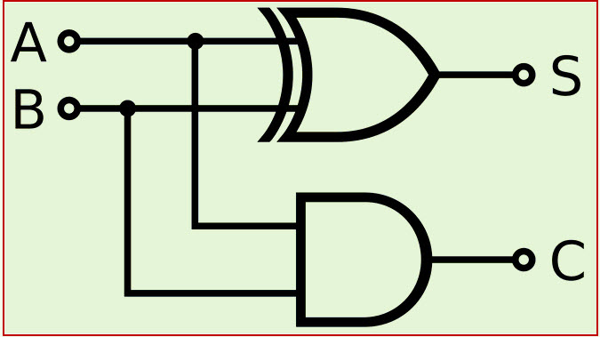
This involves from synthesis of logic to building GDSII(Graphic Data System) file, from logical schematic to layout of the chip. The physical design is vast field which has its own flow the inputs of the physical design are synthesis netlist, the output would be complete GDSII of that netlist.
So what actually physical design do? The answer to this is Physical design flow helps to convert this netlist to layout file by using several different steps like,
We will see all this physical design steps in details.
Image references
https://www.google.co.in/url?sa=i&rct=j&q=&esrc=s&source=images&cd=&cad=rja&uact=8&ved=0ahUKEwiQyZKoneXUAhXEs48KHXUdArcQjRwIBw&url=https%3A%2F%2Fwww.youtube.com%2Fwatch%3Fv%3DheCZKVI8Vf4&psig=AFQjCNGRhL1OkTMIVyU8dEdaG9UnnhRBkg&ust=1498900277226069
https://www.google.co.in/url?sa=i&rct=j&q=&esrc=s&source=images&cd=&cad=rja&uact=8&ved=0ahUKEwiP86q4neXUAhWDv48KHbU1Dq4QjRwIBw&url=https%3A%2F%2Fwww.elprocus.com%2Fhalf-adder-and-full-adder%2F&psig=AFQjCNG0AcmDBmd_8uLfHVwE7kVX4mmHhQ&ust=1498899992158197
This involves from synthesis of logic to building GDSII(Graphic Data System) file, from logical schematic to layout of the chip. The physical design is vast field which has its own flow the inputs of the physical design are synthesis netlist, the output would be complete GDSII of that netlist.
So what actually physical design do? The answer to this is Physical design flow helps to convert this netlist to layout file by using several different steps like,
- Static Timing Analysis(STA)
- Design Partitioning
- Floor Planning
- Placement
- Clock Tree Synthesis
- Routing
- Signoff(Physical Verification)
We will see all this physical design steps in details.
 |
| Layout schematic |
 |
| Logic Schematic |
Image references
https://www.google.co.in/url?sa=i&rct=j&q=&esrc=s&source=images&cd=&cad=rja&uact=8&ved=0ahUKEwiQyZKoneXUAhXEs48KHXUdArcQjRwIBw&url=https%3A%2F%2Fwww.youtube.com%2Fwatch%3Fv%3DheCZKVI8Vf4&psig=AFQjCNGRhL1OkTMIVyU8dEdaG9UnnhRBkg&ust=1498900277226069
https://www.google.co.in/url?sa=i&rct=j&q=&esrc=s&source=images&cd=&cad=rja&uact=8&ved=0ahUKEwiP86q4neXUAhWDv48KHbU1Dq4QjRwIBw&url=https%3A%2F%2Fwww.elprocus.com%2Fhalf-adder-and-full-adder%2F&psig=AFQjCNG0AcmDBmd_8uLfHVwE7kVX4mmHhQ&ust=1498899992158197